
Programmable digital resources can be used to overcome the shortcomings of SoC devices
Author: Robert Murphy Date: 2015-01-27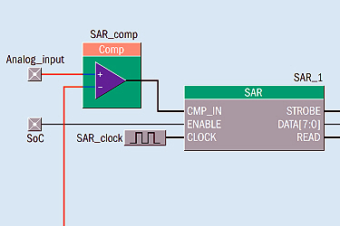
One of the most frustrating elements of embedded system development occurs when, having passed many design milestones, you discover that the embedded device selected doesn't meet current design requirements.
Configurability offers designers the flexibility to determine how peripherals such as comparators and operational amplifiers are routed out to pins. These components will not have the same static pin locations as a traditional fixed function microcontroller; using a series of registers on the device, engineers can configure a device to their particular application needs. Additionally, mixed signal SoC devices may contain digital resources that are programmable at different levels – from basic configurable logic to larger PLD resources – and which can be configured using a hardware description language such as Verilog. Using these programmable digital resources, developers can create state machines and other complex circuits, such as the ability to perform an FFT on a digital signal in hardware.
Whilst this high level of configurability allows developers to accommodate design changes that may occur during development, there are still some instances where the limitations of the chosen SoC are reached. This can happen when the design requirements exceed the capabilities of the part or when there is the need to implement a feature that does not have a fixed-function component on the silicon. By using the configurability and flexible routing that makes a mixed signal SoC so useful in the first place, developers can overcome many of the shortcomings the device architecture itself may have.
Overcoming analogue design challenges can be one of the most difficult parts of the embedded mixed signal development process. Unlike digital peripherals, which are considered to be more 'universal' and to act more like building blocks, analogue peripherals are 'fairly fixed' in their functionality as they are essentially a system of components themselves, rather than building blocks. Engineers will have access to analogue peripherals such as A/D converters, comparators and D/A converters, all of which can be configured to some level.
One design challenge that is commonly encountered is the need for an additional A/D converter in a design. This can be when the engineer does not want to multiplex an A/D converter input or would like to implement a specific type of A/D converter – an SAR converter, for example – in a device that only contains a Delta-Sigma A/D converter. To understand how a SoC can overcome this from within itself, let's look at this from the perspective of a design needing an SAR A/D converter. The components required to build a SAR A/D converter are a comparator, a D/A converter, a status register and some programmable digital logic. All these components can be found on SoC devices.
When these components are arranged in a fashion that is similar to that shown in Figure 1, a functional SAR A/D converter can be created.
The 8bit output is gathered by reading the information stored in the status register. Various digital functions, such as arithmetic operations and bit shifting, are done in hardware using Verilog. This combination of resources – capable of sampling at 118ksample/s at 8bit – has created functionality that did not previously exist in the device. As an additional benefit, as long as there are more comparators, D/A converters and digital logic, additional SAR A/D converters can be created.
Many mixed signal SoC devices also contain dedicated comparators and operational amplifiers. When those resources become exhausted, or in the case that the device never included those peripherals, what can be done? A variety of analogue circuits, such as comparators, active filters, programmable gain amplifiers, or transimpedance amplifiers, are all comprised of an operational amplifier that uses various resistors and/or capacitors to create a specific function. Some mixed signal SoCs contain switched capacitor (SC) peripherals. These are built around low noise, low offset op amps surrounded by analogue multiplexers, themselves surrounded by groups of capacitors and switches. If the switches are put into a static open or closed state, this results in a capacitor attached to the circuit. In addition, if the switches (?1 and ?2 in Figure 2) are opened and closed alternatively at a given frequency, the switched capacitor begins to behave like a lossless resistor.
Devices that incorporate switched capacitors, such as the PSoC family of devices from Cypress Semiconductor, use register configuration to control the switches in the switch capacitor topology to produce a variety of circuits, from the basic operational amplifier to more advanced circuits, such as a mixer, integrator or tack and hold.
Developers face significant digital design challenges with SoC architectures. If you look at a traditional microcontroller, they will contain some fixed function digital peripherals, such as PWMs and timers. SoC devices incorporate digital logic, similar to the block diagram shown in fig 3. Using hardware description languages such as Verilog, these hardware resources can be configured to work together to create a range of functional components.
Consider a SoC device that contains a peripheral USB interface. It may be decided late in the design cycle that it would be beneficial to also support host USB capabilities to support such features as allowing a USB flash drive to be connected for data logging or field programmable firmware updates. The problem is that the device being used does not contain the required hardware to implement host functionality. However, using the configurable digital resources, a SoC device can overcome this digital design limitation.
In order to understand what needs to be incorporated, the engineer has to start by thinking about what it takes to handle USB communication. There are the differential signals, then SOF generation, NRZI encoding/decoding, CRC calculating, bit stuffing and IN/OUT packet parsing with some extensive Verilog coding to use the digital resources shown in fig 3. Individual components for host USB communication can be created, with each block representing a Verilog implementation with various digital inputs and outputs. By connecting these components together with some glue logic, along with the addition of some external pull down resistors and a crystal oscillator, a fully functional USB host can be implemented.
Such configurability means that if a mixed signal SoC selected for a design contains, for example, two PWMs, two comparators, two D/A converters and a Delta-Sigma A/D converter, these peripherals are not the end of its hardware functionality. Resources can be repurposed and modified to extend resources to provide functionality beyond that which may have been initially required.
In this way, engineers can increase the value of a product as well as reduce development time of a new product design without having to migrate to a new embedded device, avoiding the need for new firmware development and PCB layout, lost time and money. By calling upon skills learned in early electrical engineering classes, combined with the flexibility of mixed signal SoC device, you can efficiently compensate for the shortcomings of your SoC.
Author profile
Robert Murphy is a systems engineer with Cypress Semiconductor
From: http://www.newelectronics.co.uk/